Every time you save a document, take a photo, or download an app on your computer, smartphone, or tablet, you’re relying on an amazing piece of technology: the floating gate transistor. These are the fundamental building blocks of NAND flash memory, the storage medium that powers modern solid-state drives (SSDs).
Unlike volatile memory found in RAM, floating gate transistors can retain stored data even when power is disconnected, making them ideal for permanent data storage. This non-volatile characteristic is what allows your devices to remember your files, photos, and applications even after being powered off for extended periods.
This comprehensive guide explores how floating gate transistors work, their role in modern storage technology, and why they’ve become the backbone of today’s digital storage solutions.
What is a Floating Gate Transistor?
Basic Concept
Think of a floating gate transistor as an intelligent memory cell that can remember information indefinitely without power. Unlike a traditional light switch that forgets its position when unplugged, a floating gate transistor maintains its state—storing either a ‘1’ or ‘0’—even when electricity is removed.
Physical Structure
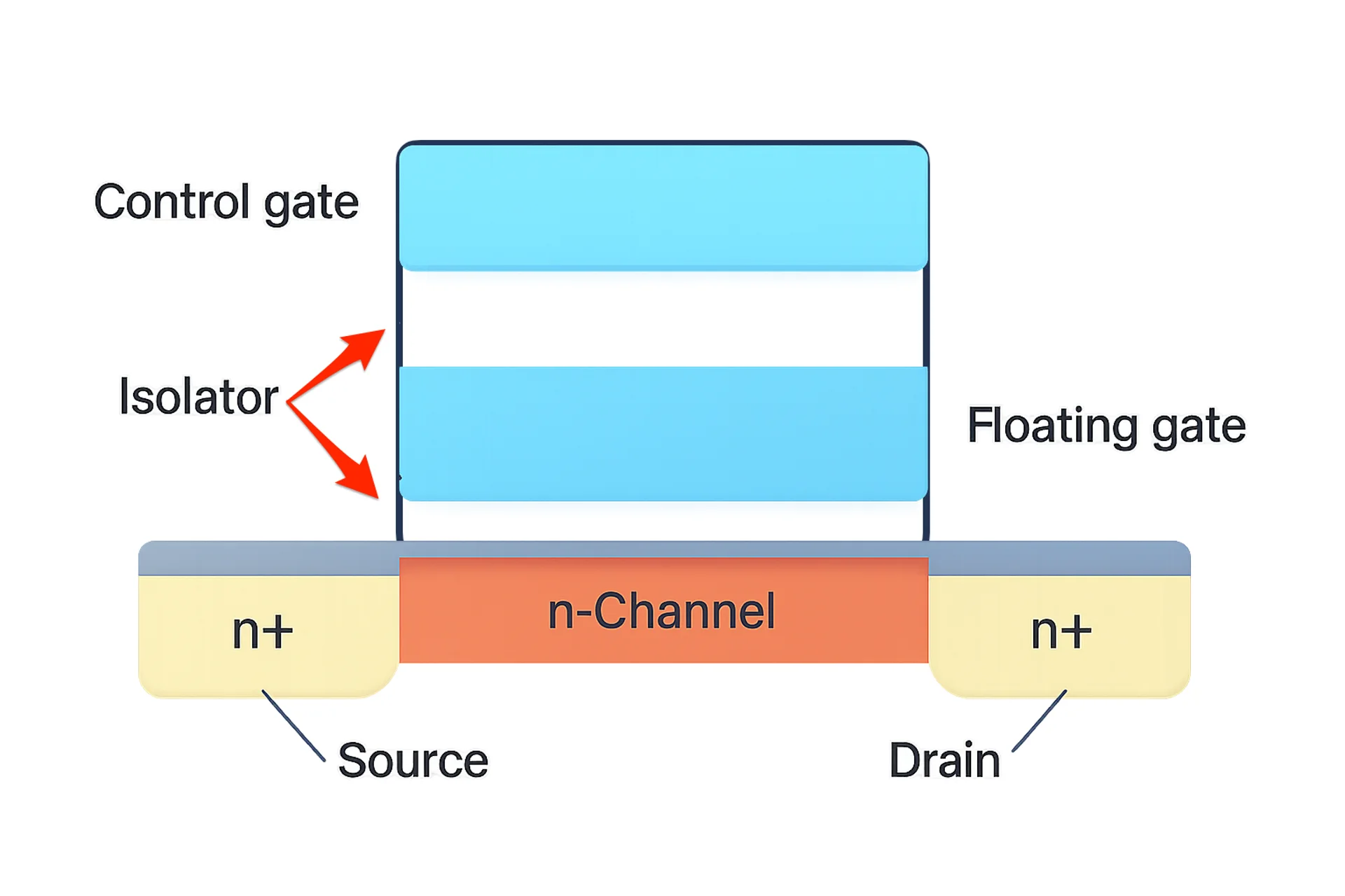
A floating gate transistor consists of several key components:
- Control Gate: The top electrode that controls the transistor’s operation
- Floating Gate: A conductive layer (typically polysilicon) completely surrounded by insulating oxide material
- Source and Drain: The terminals between which current flows
- Oxide Layers: Thin insulating layers that trap electrical charges
The floating gate is the critical component. It’s electrically isolated (which is what “floating” means in this context) and can trap electrical charges for years, decades, or even longer without requiring power to maintain the stored information.
As you probably already know, data is stored in the form of ones and zeros. By controlling the amount of electrical charge trapped in the floating gate can represent either one of these two states. Binary ‘1’ is represented when there is no charge or minimal charge in the floating gate, whereas a binary ‘0’ is when significant charge is trapped in the floating gate
The presence or absence of charge changes the transistor’s threshold voltage (the minimum voltage needed to turn the transistor “on” and allow current to flow).
Operating Principles
Charge Storage Mechanism
The ability to store and retain electrical charge is what sets floating gate transistors apart from other types of transistors. When charges are stored in the floating gate, they modify the transistor’s electrical behavior, specifically its threshold voltage. This change serves as the basis for data storage.
The trapped charges can remain stable for years due to the insulating oxide layers that completely surround the floating gate, creating an effective barrier that prevents charge leakage.
Reading Data
Reading data from a floating gate transistor involves applying a specific voltage to the control gate and measuring the resulting current flow:
- Apply Test Voltage: A predetermined voltage is applied to the control gate
- Measure Current: The system measures whether current flows between source and drain
- Interpret Result:
- If current flows easily → Low threshold voltage → Data is ‘1’
- If current doesn’t flow or flows weakly → High threshold voltage → Data is ‘0’
Writing and Erasing Data
Two primary mechanisms are used for modifying the charge in floating gate transistors:
Hot Electron Injection (Writing Data)
- Used to add electrons to the floating gate (programming to ‘0’)
- High-energy electrons overcome the oxide barrier and become trapped
- Creates a higher threshold voltage state
Fowler-Nordheim Tunneling (Erasing Data)
- Used to remove electrons from the floating gate (erasing to ‘1’)
- Quantum mechanical process that allows electrons to tunnel through the oxide barrier
- More efficient and less damaging to the oxide layer than other methods
- Primarily used for block-level erasure operations
Multi-Level Cell Technology
Beyond Single-Bit Storage
Early implementations stored only one bit per cell (Single-Level Cell or SLC). SSDs using this technology were in some ways superior to modern variations, as it offer better performance (low latency) and improved durability for the NAND flash. Today, there are additional charge levels.
| Characteristic | SLC (Single-Level Cell) |
MLC (Multi-Level Cell) |
TLC (Triple-Level Cell) |
QLC (Quad-Level Cell) |
|---|---|---|---|---|
| Capacity | 1 bit per cell | 2 bits per cell | 3 bits per cell | 4 bits per cell |
| States | 2 (charged/uncharged) |
4 distinct charge levels |
8 distinct charge levels |
16 distinct charge levels |
| Reliability | Highest | Good | Adequate for consumer use |
Lowest |
| Cost | Most expensive | Moderate | Lower | Cheapest |
| Typical P/E Cycles | 50,000-100,000 | 3,000-10,000 | 500-3,000 | 100-1,000 |
Why TLC Dominates Consumer SSDs
TLC NAND has become the most popular choice for consumer SSDs because it offers an optimal balance of storage storage density, cost effectiveness (it’s significantly cheaper than SLC and MLC, solid performance, but also better reliability compared to QLC.
SSD Architecture and Scale
Understanding the Numbers: 1TB TLC SSD Structure
To appreciate the scale of modern SSDs, let’s break down a typical 1TB TLC NAND SSD:
Basic Calculations
- Total Capacity: 1TB = 1,099,511,627,776 bytes = 8,796,093,022,208 bits
- Bits per Cell: 3 (TLC)
- Total Cells: 8,796,093,022,208 ÷ 3 = 2.93 trillion floating gate transistors
Organizational Structure
- Page Size: Typically 16KB (smallest read/write unit)
- Block Size: Typically 256 pages (smallest erase unit)
- Total Pages: ~67 million
- Total Blocks: ~262,000
3D NAND Technology
Modern SSDs use 3D NAND technology, which stacks memory cells vertically to increase density. Layer count is currently (2025) well above 200 for high-end SSDs. This dramatically increases storage capacity without expanding the physical footprint. Manufacturing is more complex but enables higher densities and better cost per gigabyte
Advantages of Floating Gate Technology
Why Floating Gates Dominate SSD Storage
- Non-Volatile Storage: Retains data without power
- High Density: Excellent storage capacity per unit area
- Fast Access: Quick read and write operations
- Energy Efficiency: Low power consumption compared to volatile alternatives
- Proven Technology: Mature manufacturing processes and reliability
- Cost Effective: Economical for mass production
Performance Characteristics
- Read Speed: Very fast, typically limited by interface rather than cell speed
- Write Speed: Good, though slower than reads due to programming complexity
- Endurance: Varies by cell type, but adequate for intended applications
- Data Retention: Years to decades without power
Alternative Storage Technologies
While floating gate transistors dominate current SSD technology, several alternatives are being developed:
Charge Trap Flash (CTF)
- Mechanism: Uses insulating nitride layer instead of conductive floating gate
- Advantages: Better durability, improved data retention, potentially lower costs
- Status: Increasingly adopted in modern high-density applications
3D XPoint (Intel Optane)
- Principle: Changes material resistance to store data
- Advantages: Lower latency, higher endurance than NAND
- Limitations: Higher cost, limited availability
MRAM (Magnetoresistive RAM)
- Principle: Uses magnetic states for data storage
- Advantages: Extremely durable, excellent retention
- Limitations: Higher manufacturing cost
ReRAM (Resistive RAM)
- Principle: Changes resistance in solid dielectric materials
- Potential: High density, low power consumption
- Status: Still in development phase
Phase-Change Memory (PCM)
- Principle: Uses material phase changes (amorphous to crystalline)
- Advantages: Good retention and speed
- Limitations: Higher production costs
Floating Gate vs. Charge Trap: A Detailed Comparison
| Feature | Floating Gate | Charge Trap |
|---|---|---|
| Structure | Conductive polysilicon gate surrounded by oxide | Insulating nitride trapping layer |
| Charge Storage | In conductive floating gate | In insulating trap sites |
| Data Retention | Good, can degrade over time | Generally superior due to better insulation |
| Durability | Sensitive to oxide wear | More resistant to degradation |
| Manufacturing | More complex process | Simpler, potentially cheaper |
| Scalability | Challenging at smaller sizes | Better scaling to smaller geometries |
| Error Rates | Low with proper error correction | Generally lower due to better charge confinement |
| Energy Efficiency | Good, but some leakage possible | Better due to improved insulation |
Limitations and Challenges
Program/Erase Cycle Limits
Each write/erase cycle causes microscopic damage to the oxide layers, limiting the transistor’s lifespan. This is why SSDs implement:
- Wear Leveling: Distributes writes evenly across all cells
- Over-Provisioning: Extra capacity to replace worn-out cells
- Error Correction: Advanced algorithms to maintain data integrity
Write Amplification
The requirement to erase entire blocks before writing new data can lead to write amplification, where more data is actually written to the NAND than requested by the host system.
Scaling Challenges
As manufacturing processes shrink to smaller nodes, maintaining reliable charge storage becomes increasingly difficult due to:
- Reduced oxide thickness
- Increased interference between adjacent cells
- Higher error rates requiring more sophisticated error correction
Summing Up
Floating gate transistors represent one of the most successful and widely deployed storage technologies in modern computing. Their ability to reliably store data without power, combined with excellent performance characteristics and cost-effectiveness, has made them the foundation of the digital storage revolution.
From smartphones to enterprise data centers, billions of these microscopic devices work continuously to preserve our digital lives. As we generate and consume ever-increasing amounts of data, floating gate transistors continue to evolve, becoming denser, more reliable, and more efficient.
As we look toward the future, floating gate transistors will likely remain a critical component of our digital infrastructure, even as new technologies emerge to complement and enhance their capabilities.
Frequently Asked Questions
Q: How long do floating gate transistors typically last in consumer SSDs?
A: The lifespan varies by NAND type: SLC can handle 50,000-100,000 P/E cycles, while TLC typically manages 500-3,000 cycles. With wear leveling and over-provisioning, consumer SSDs often last 5-10 years under normal usage.
Q: Why don’t SSDs use only SLC NAND if it’s more reliable?
A: SLC is significantly more expensive to manufacture and has lower storage density. TLC and QLC provide better cost per gigabyte while offering sufficient reliability for most consumer applications.
Q: Can floating gate transistors be used for applications other than storage?
A: Yes, they’re used in analog signal processing, hardware security modules, timers, oscillators, and various sensor applications where non-volatile programmable behavior is needed.
Q: What makes SSDs more power-efficient than traditional hard drives?
A: SSDs have no moving parts and floating gate transistors consume minimal power. They only use significant energy during active read/write operations, unlike hard drives which continuously power motors and actuators.
Q: How does 3D NAND improve upon traditional planar NAND?
A: 3D NAND stacks memory cells vertically, dramatically increasing storage density without requiring smaller manufacturing processes. This approach also often improves reliability by using larger individual cells while achieving higher overall capacity.