
While the tech industry grapples with a deepening memory supply crunch due to the AI bubble, South Korean memory giant SK Hynix is moving forward with High Bandwidth Storage (HBS) – a technology that stacks DRAM and NAND chips to eliminate performance bottlenecks for mobile AI processing in particular.
HBS is said to solve a fundamental problem: as on-device AI becomes standard in smartphones, existing storage architectures can’t keep pace with the computational demands. According to ETNews (in Korean), the company plans to stack up to 16 layers of low-power wide I/O DRAM together with NAND, interconnecting them through Vertical Wire Fan-Out (VFO) technology to improve data processing speeds.
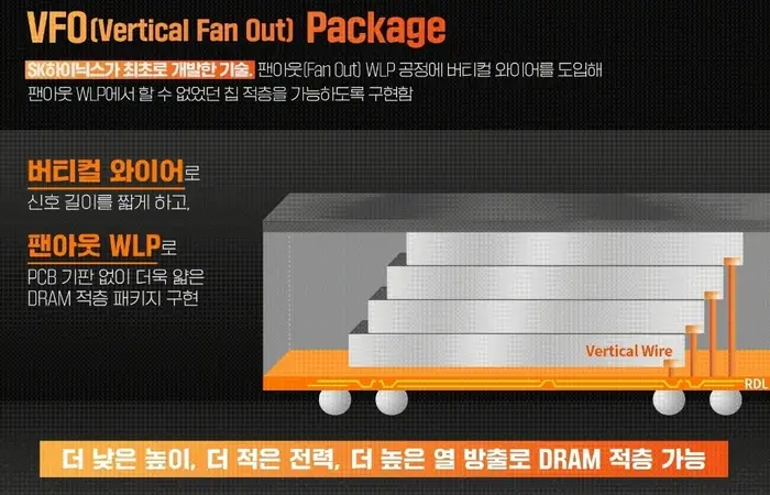
The secret to HBS is SK Hynix’s VFO packaging approach, which the company first introduced in 2023. Unlike traditional wire bonding that curves connections between chips, VFO connects stacked DRAM and NAND in straight vertical lines. This architectural shift delivers measurable gains: wire lengths shrink by 4.6 times compared to conventional designs, translating to a 4.9% improvement in power efficiency. The technology also reduces packaging height by 27% and enhances heat dissipation by 1.4%.
“VFO is an innovative next-generation packaging solution,” an SK Hynix official explained to TrendForce. “By combining traditional wire bonding with advanced Fan-Out Wafer-Level Packaging technology, we can minimize manufacturing costs without using TSV.”
That last detail matters significantly. High Bandwidth Memory (HBM), which has become essential for AI data centers, requires Through-Silicon Via (TSV) processes that penetrate the chip—an expensive manufacturing step. Because HBS doesn’t need TSV, SK Hynix can achieve higher yields and lower production costs. For smartphone and tablet manufacturers watching their margins compress, this cost advantage could prove critical.
Packaging for On-Device AI Performance
HBS will be packaged directly with an application processor and integrated into mobile device logic boards. While SK Hynix hasn’t announced which chipsets will support the technology first, the rumored Snapdragon 8 Elite Gen 6 Pro – expected to support both LPDDR6 and UFS 5.0 storage – would be a prime candidate.
Apple has reportedly looked at similar high-performance memory technologies for future iPhones, for the purpose of running more intensive AI models locally rather than relying on cloud processing. As voice assistants, real-time translation, and generative AI features become standard smartphone capabilities, the storage bottleneck becomes more pronounced.
SK Hynix’s Broader AI Memory Strategy
HBS fits within SK Hynix’s larger vision to become a full-stack AI memory provider. At its SK AI Summit 2025 in November, the company unveiled an roadmap featuring custom HBM, AI-optimized DRAM (AI-D), and next-generation NAND Flash (AI-N).
The AI-N initiative targets next-gen storage through a three-pronged approach: AI-N P (Performance) focuses on ultra-high-speed performance; AI-N B (Bandwidth) enhances bandwidth through advanced stacking technologies to overcome HBM’s capacity limits; and AI-N D (Density) aims to deliver ultra-high-capacity solutions that improve cost competitiveness in large-scale AI storage environments.
SK Hynix is also collaborating with SanDisk to develop High Bandwidth Flash (HBF), which enhances HBM with NAND for AI inference workloads. The two companies signed a memorandum of understanding in August 2025 to jointly define HBF technical specifications and promote standardization. Samples of the actual product are expected in the second half of 2026, whereas the first AI inference systems using HBF may appear in early 2027.